Views: 80 Author: Site Editor Publish Time: 2020-06-08 Origin: Site
Introduction
A ball grid array (BGA) is a type of surface-mount packaging used for integrated circuits. BGA packages are used to permanently mount devices such as microprocessors. A BGA can provide more interconnection pins than can be put on a dual in-line or flat package, each pin is provided with a solder ball. All connections are distributed in a uniform surface grid or matrix on the component. The whole bottom surface of the device can be used instead of just the perimeter.
The leads are also on average shorter than with a perimeter-only type, leading to better performance at high speeds. Soldering of BGA devices requires precise control and is usually done by automated processes. BGA devices are not suitable for socket mounting.
Classification of BGA
According to the different substrates, it can be divided into 3 types as following:
✅PBGA (Plastic Ball Grid Array)
✅CBGA (Ceramics Ball Grid Array)
✅TBGA (Tape Ball Grid Array)
PBGA
PBGA, short for plastic ball grid array has received the widest focus and applications. With BT (bismaleimide triazine) resin used as substrate material, together with the application of sealant technologies of OMPAC (over molded pad array carrier) or GTPAC (glob to pad array carrier), the reliability of PBGA has been verified by JEDEC Level-3. Up to now, PBGA packages containing 200 to 500 solder balls are widely applied, working best for double-side PCBs.

CBGA
As is its name defined, CBGA (ceramic ball grid array) packages take advantage of ceramic as substrate material and tin balls (ratio between tin and lead: 10:90) with high melting point. Internal chip depends on C4 (Controlled Collapse Chip Connection) for perfect connection between BGA and PCB. This type of connection features excellent thermal conductivity and electrical performance. Furthermore, CBGA holds excellent reliability but with high cost. Therefore, CBGA packages are more suitable for automotives or high efficiency chips.

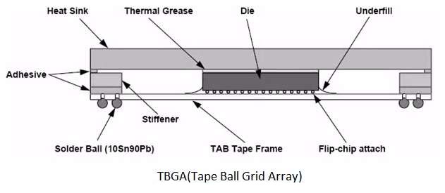
TBGA
TBGA, short for tape ball grid array, is capable of effectively shrinking package thickness and providing excellent electrical performance. Moreover, excellent thermal dissipation effect can be obtained when heat sink and chip face down design are applied. Thus, TBGA works suitably for high-efficiency products with thin packages. For chips facing down, flip chip technology should be selected while for chips facing up, wire bond should be selected. Generally speaking, TBGA features higher cost than PBGA.
Following are the advantages of BGA:
✅It will not have problem with soldering process having high density packages as solder is applied to the package in right proportion.
✅This package prevent chips from over-heating due to low thermal resistance between package and PCB because of discrete leads.
✅BGA is used in security sensitive applications as it prevents direct physical access to the chip.
✅It provides very short distance between PCB and package. Hence it offers low inductance and consecutively superior performance compare to leaded devices.
Following are the disadvantages of BGA:
✅The solder balls can not flex in the same way as longer leads can.
✅After soldering, it is very difficult to look for faults, Moreover it requires expensive tools such as X-ray machines and specially developed microscopes to do it.
Conclusion
Now that so many classifications of BGA are available, optimal BGA packages should be picked up based on the properties of your final products, your cost limitations and expected performance and functions. Onlitex provides professional suggestions on your optimal type of BGA components taking above elements into full consideration. Furthermore, 100% components have to be checked prior to their applications to ensure their perfect performance will be obtained in final products.