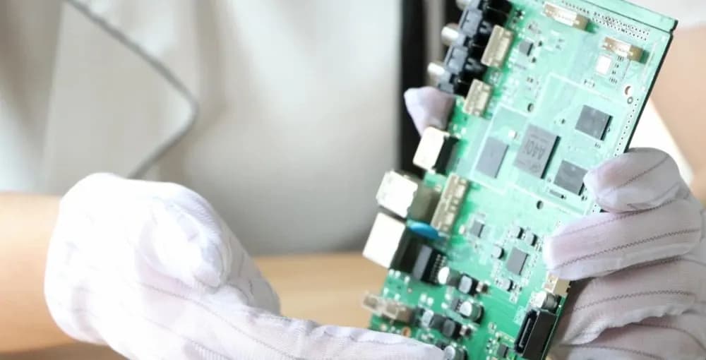
What OSP is, how the OSP surface finish is applied step by step, the process parameters that control film quality, and the limitations to plan for.
 Onlitex Engineering Team3 min read
What is OSP?
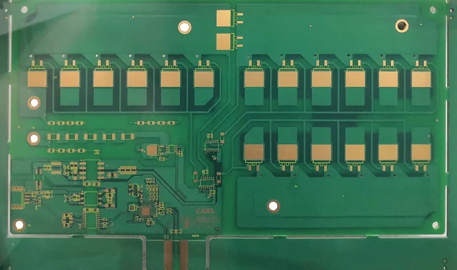
OSP is short for organic solderability preservative. It is also called an organic solder protective film or copper protector, and it is also known as preflux. Simply put, OSP is an organic film grown chemically on a clean, bare copper surface.
The film resists oxidation, thermal shock and moisture, protecting the copper surface from further corrosion (oxidation, sulfurization and so on) in a normal environment. During the high temperatures of subsequent soldering, however, the protective film must be removed quickly and easily by the flux, so that the exposed clean copper can immediately combine with the molten solder and form a solid solder joint in a very short time.
Advantages and history of OSP
OSP is not a new technology. It has been around for over 35 years, longer than SMT. OSP has many advantages:
- Good flatness
- No IMC (intermetallic compound) forms between the copper and the pad finish, so the solder bonds directly to the copper during soldering (good wettability)
- A low-temperature process
- Low cost, which can be lower than HASL
- Low energy consumption during processing
In its early days, OSP was very popular in Japan, where about 40% of single-sided boards and nearly 30% of double-sided boards used it. In the United States, OSP use surged after 1997, rising from about 10% before 1997 to 35% in 1999.
Types of OSP
There are three major categories of OSP material: rosin, active resin and azole. The most widely used today is azole OSP, which has been improved over about five generations, named BTA, IA, BIA, SBA and, most recently, APA.
The OSP process flow
The process flow for applying OSP to a PCB is:
- Degreasing
- Two-stage water rinse
- Micro-etching
- Two-stage water rinse
- Acid washing
- DI water rinse
- Film forming and air drying
- DI water rinse
- Drying
Degreasing
The effectiveness of degreasing directly affects the quality of film formation, and poor degreasing results in uneven film thickness. On the one hand, the concentration can be kept within the process range by analyzing the solution. On the other hand, the degreasing effect should be checked regularly, and if it is not good enough, the degreasing solution should be replaced promptly.
Micro-etching
The purpose of micro-etching is to roughen the copper surface so that the film forms easily. The micro-etching depth directly affects the film formation rate, so keeping it stable is very important for a stable film thickness. It is generally appropriate to control the micro-etching depth between 1.0 and 1.5 µm. Before each production shift, the micro-etching rate can be measured and the micro-etching time set accordingly.
Film forming
It is best to rinse with DI water before film forming to prevent contamination of the film-forming solution. A DI water rinse is also recommended after film forming, with the pH controlled between 4.0 and 7.0 to prevent contamination and damage to the film.
The key to the OSP process is controlling the thickness of the anti-oxidation film. If the film is too thin, it has poor heat and impact resistance and cannot withstand the high temperatures of reflow soldering (190–200 °C), which ultimately affects soldering performance. If it is too thick, the flux on the assembly line cannot dissolve it well, which also affects soldering performance. It is generally appropriate to control the film thickness between 0.2 and 0.5 µm.
Disadvantages of OSP
OSP also has its shortcomings:
- Actual formulas vary widely, and so does their performance, so suppliers must be carefully qualified and selected.
- The protective film is extremely thin and easily scratched, so boards must be handled with care.
- After several high-temperature soldering cycles, the OSP film on pads that have not yet been soldered may discolor or crack, affecting solderability and reliability.
- The solder paste printing process must be well controlled, because misprinted boards cannot be cleaned with IPA or other methods without damaging the OSP layer.
- The transparent, non-metallic OSP layer is difficult to measure, and its coverage is not easy to see, so it is hard to evaluate the quality stability of suppliers in these respects.
- OSP provides no IMC barrier between the Cu in the pad and the Sn in the solder. In lead-free soldering, the SnCu intermetallic in high-tin solder joints grows quickly, which affects solder joint reliability.
For a side-by-side comparison with another common finish, see HASL vs OSP.
- #OSP
- #PCB surface finish
- #lead-free soldering