How automated optical inspection (AOI) works on PCB assemblies, why it replaced manual inspection, and the defects it detects on assembled and bare boards.
 Onlitex Engineering Team1 min read
PCBA Automated Optical Inspection (AOI) Explained
What is automated optical inspection?
Automated optical inspection (AOI) is a machine-based technique used to test and evaluate PCBs for potential faults such as surface defects, dimensional defects and component placement defects. As circuits become more complex, manual inspection of boards has become almost impossible, so AOI plays an important role in checking printed circuit boards after assembly. Because it is automated, AOI helps achieve the desired product quality on the production line while keeping costs as low as possible.
How AOI works
The inspection starts with a visual scan of the board. The captured image of the board is then compared with the ideal board image that has been entered into the AOI machine.
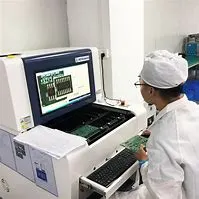
The board is placed under bright light sources, such as fluorescent, LED, infrared or ultraviolet lighting, with one or more high-definition cameras. This is how the AOI machine captures the picture of the PCB. Processing software then compares the captured picture with the stored information about what the board should look like, and after this comparison, AOI highlights the defects.
What defects can AOI detect?
AOI can detect surface defects such as nodules and scratches, and dimensional defects such as open circuits, shorts and solder thinning. It can also detect wrong components, missing components and incorrectly placed components.
Assembled boards (SMT inspection)
For a PCB with components, AOI can detect:
- Area defects
- Billboarding
- Component offset
- Component polarity
- Component presence or absence
- Component skew
- Excessive solder joints
- Flipped components
- Height defects
- Insufficient paste around leads
- Insufficient solder joints
- Lifted leads
- No-population tests
- Paste registration
- Severely damaged components
- Tombstoning
- Volume defects
- Wrong parts
- Solder bridging
Bare PCBs
For a bare PCB, AOI can detect:
- Line width violations
- Spacing violations
- Excess copper
- Missing pads
- Short circuits
- Cuts
- Hole breakage (a via going outside its pad)
- Incorrect mounting of components
Learn more about our inspection and testing services.
- #AOI
- #PCBA inspection
- #quality control
- #SMT defects