What an SMT stencil is, why PCB assembly relies on it to deposit the right amount of solder paste on each pad, and why stencil apertures are electropolished.
 Onlitex Engineering Team1 min read
Why Does PCBA Need a Stencil?
What is a PCB stencil?
A PCB stencil is a sheet of stainless steel with laser-cut openings, used to apply solder paste to a PCB for surface-mount component placement. The stencil deposits solder paste at designated places on the bare PCB so that components can be placed and perfectly aligned on the board.
Why PCB assembly needs a stencil
The stencil's main function is to deposit exactly the right amount of solder paste on the SMT pads, so that the solder joint between each pad and component is perfect in terms of both electrical connection and mechanical strength.
Using a PCB stencil to apply solder paste makes the PCB assembly process faster, and it also makes it easier to apply solder paste accurately.
Electropolishing the apertures
During stencil making, the aperture walls become rough because of the constant application of the laser beam. The laser melts the sheet material, which leaves surface irregularities called micro-burrs on the aperture walls. To solve this problem, the stencil is electropolished to smooth the aperture walls. This helps the solder paste transfer easily from the stencil to the intended PCB pads.
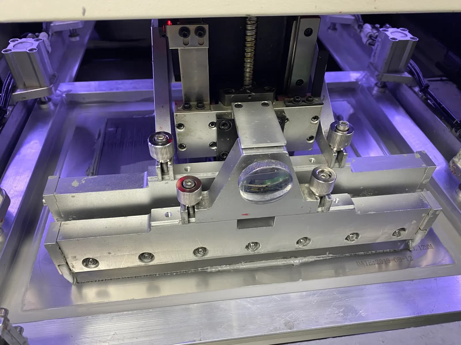
To see how the squeegee pushes paste through the stencil, read about the influence of the squeegee system on PCBA processing.
- #SMT stencil
- #solder paste printing
- #PCB assembly