What makes high density interconnect (HDI) PCBs different, the advantages of microvias and dense routing, and where HDI boards are used today.
 Onlitex Engineering Team2 min read
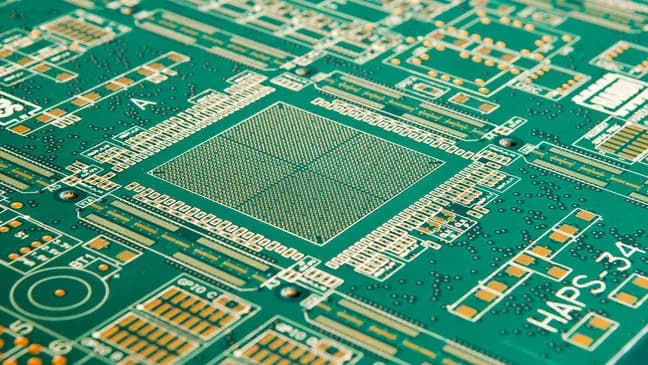
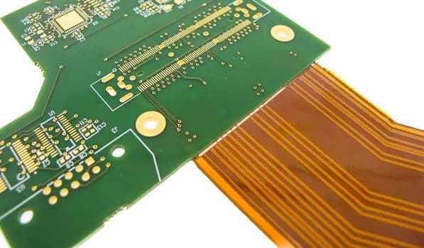
High density interconnect (HDI) PCB is one of the fastest-growing technologies in printed circuit boards. HDI boards have a higher circuit density than conventional circuit boards: they combine smaller vias and capture pads with a higher connection pad density. HDI boards contain blind and buried vias and usually use microvias with a diameter of 0.006 in (0.15 mm) or less.
With HDI technology, designers can place more components on both sides of the board. With the development of via-in-pad and blind-via technologies, designers can put smaller components closer together, which means faster signal transmission and a significant reduction in signal loss and delay. The sections below outline the main benefits of HDI PCBs and where they are used.
Advantages of HDI PCBs
- Lower power consumption, which extends the battery life of the devices they power.
- More components in a restricted area. HDI boards are more densely populated, with denser trace routing.
- Durability, with increased strength and fewer drilled holes.
- Room to grow. Unlike traditional PCBs, additional components can be added as requirements change.
- Compact and lightweight boards.
- Fast signal transmission with improved signal quality.
Applications of HDI PCBs
HDI PCBs are found in mobile phones, touch-screen devices, laptop computers, digital cameras and 4G network communications, and they are also prominent in medical devices.
Communications
Routers, semiconductors, switches and modules rely heavily on HDI PCBs. Computerized gadgets, electronic communications equipment and radio-frequency designs are very likely to use HDI boards. Audio and video devices also take full advantage of HDI PCBs, and these high-tech boards support the networks used by business and everyday communications.
Consumer electronics
Without HDI PCBs, the journey from the mainframe computer to the palmtop would have been impossible. A compact gadget such as a smart watch can perform many of the functions of a smartphone and a computer, and HDI is a big part of the reason. Beyond smartphones, tablets, laptops and wearable devices, HDI PCBs have become standard in Internet of Things products for the home, such as refrigerators, smart TVs and thermostats.
Medical equipment
HDI PCBs play an important role in modern medicine. Hospital equipment for imaging, monitoring, laboratory analysis and surgery is driven by these boards. High-density designs make devices smaller and more cost-effective while improving their performance, which helps improve the accuracy of medical testing and monitoring.
Automotive and aerospace
Most vehicles today run on computer-controlled systems. The latest models are equipped with around 50 microprocessors that handle engine control, diagnostics, safety functions and more. On-board GPS and Wi-Fi, parking sensors and rear-view mirrors also depend on HDI PCBs. As the automotive industry develops, the role of HDI PCBs will only become greater.
Conclusion
HDI PCBs are taking the industry by storm and are becoming the clear alternative to conventional PCBs wherever size, weight and signal performance matter.
- #HDI PCB
- #microvias
- #PCB design