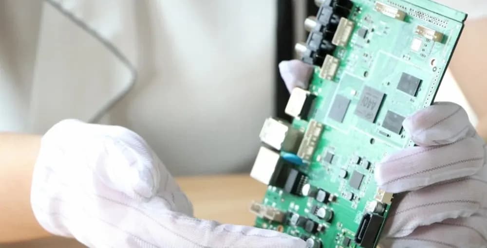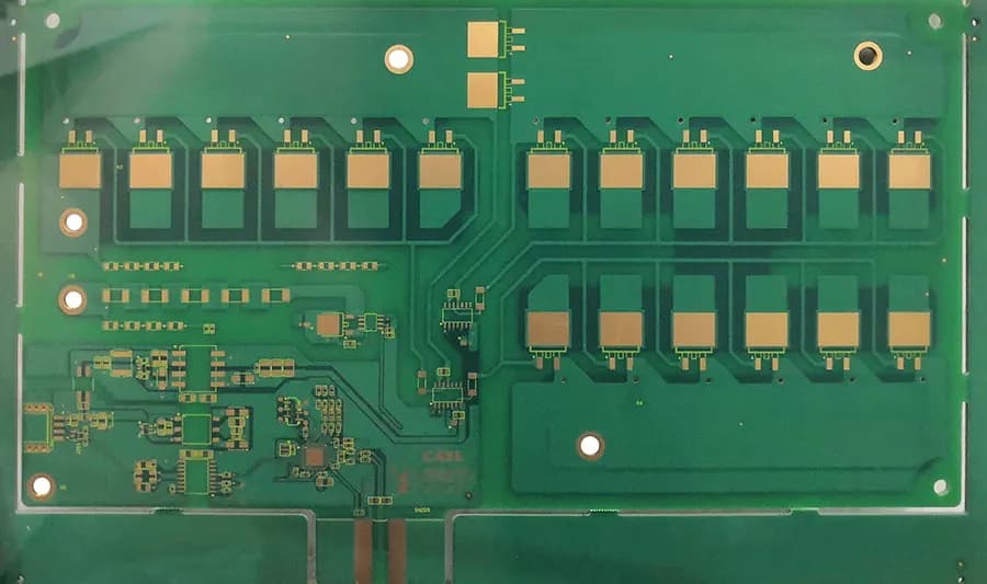
The main steps in making a bare PCB, from material cutting and drilling to imaging, etching, solder mask, V-cut, routing, electrical testing and OSP.
 Onlitex Engineering Team2 min read
The PCB Manufacturing Process, Step by Step
Below are the main steps in manufacturing a bare PCB, with the points to watch at each stage. Several of the notes refer to aluminum-based boards, where the aluminum substrate needs extra care.
1. Material cutting
Cut the large laminate sheets to the size required for production. When cutting, check the dimensions of the first piece and watch out for scratches on the surface.
2. Drilling
Drilling positions the holes in the board, which supports the subsequent production processes and the customer's assembly. Check the number and size of the holes, check the aluminum surface for drilling damage, and check for hole offset.
3. Dry/wet film imaging
The dry/wet film imaging process is: board scrubbing → film application → exposure → developing.
4. Acid/alkaline etching
The acid/alkaline etching process is: etching → film stripping → drying → board inspection.
After dry/wet film imaging, the required circuit areas are protected and the excess copper outside the circuit is etched away. During acid etching, watch for corrosion of the aluminum substrate by the etching solution. Also pay attention to undercutting, over-etching, line width and circuit layout.
5. Solder mask and legend printing
The solder mask protects circuits that do not need soldering and prevents solder from bridging and causing short circuits, while the legend (silkscreen) characters mark the board. The process is: screen printing → pre-baking → exposure → developing → legend printing.
6. V-cut and routing
The process is: V-cut → routing → peel off the protective film → remove waste material.
- V-cut: cuts part-way through the panel along the outline of each single board, so the boards are easy to package, separate and use.
- Routing: removes the excess material around the circuit board.
7. Testing and OSP
The process is: circuit test → withstand voltage test → OSP.
- Circuit test: checks whether the finished circuit works normally.
- Withstand voltage test: checks whether the finished circuit can withstand the specified voltage.
- OSP: improves the solderability of the circuit.
Need PCBs or PCB assembly?
The above is an introduction to bare PCB manufacturing. If you have an order for any PCBs, email us. Onlitex is a professional PCBA manufacturer that provides PCB solutions for electronics companies around the world.
- #PCB manufacturing
- #PCB fabrication
- #aluminum PCB